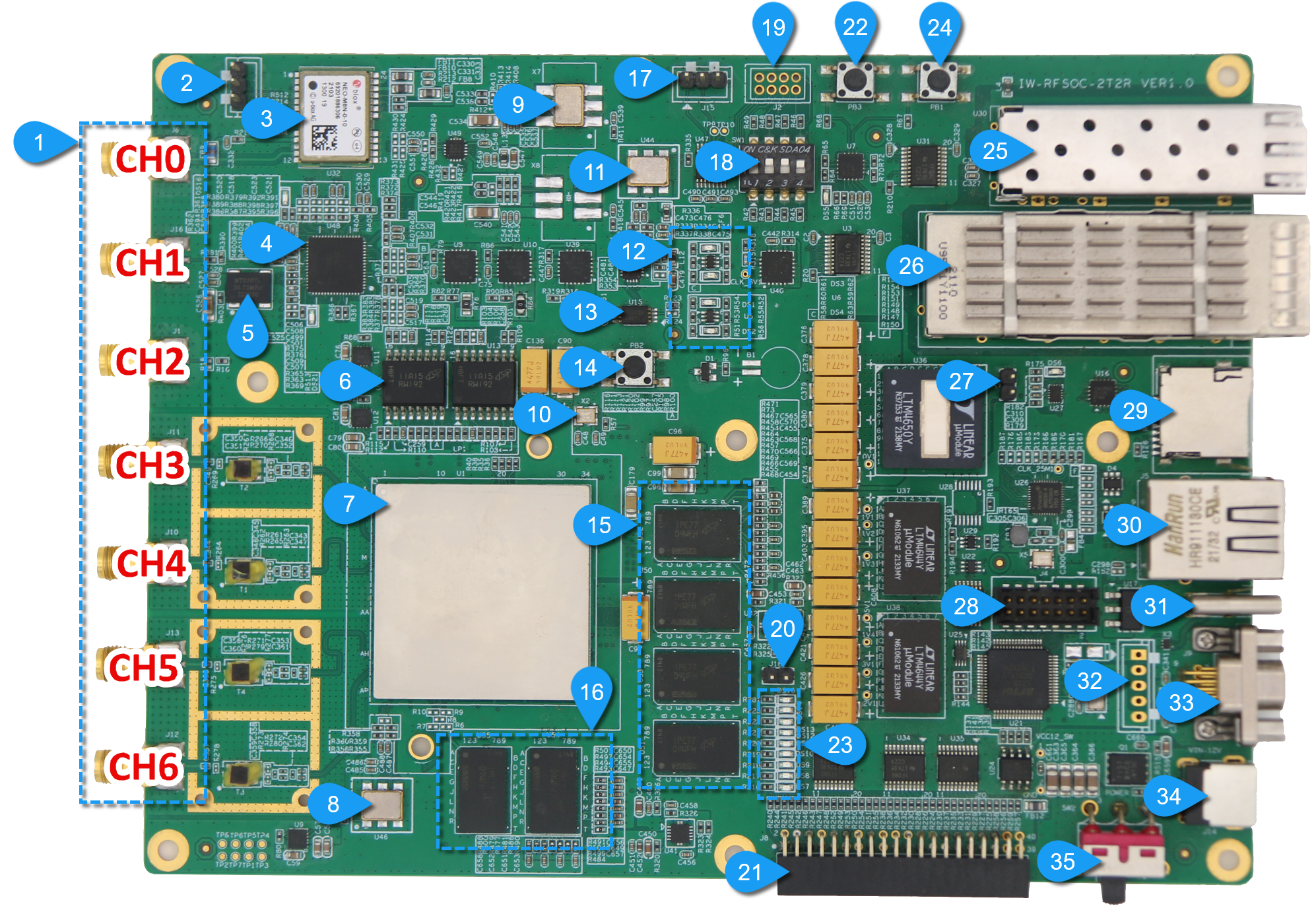
¶ Board Overall Structure
¶ Board Functions and Locations
| Number | Function |
|---|---|
| 1 | SMA interface group, numbered CH0-6 from top to bottom. CH0 is GPS signal port; CH1 is external reference clock input port; CH2 is GPIO port; CH3-6 are RF-ADC/DAC interfaces. |
| 2 | GPS module's USB debug port, from top to bottom: GND, DN, DP. |
| 3 | GPS module. |
| 4 | Clock tree chip. |
| 5 | 30.72MHz crystal oscillator, used to provide reference clock for the clock tree. |
| 6 | QSPI nor Flash chipset in dual_parallel mode, total capacity 2Gbit (256MByte). |
| 7 | Xilinx Zynq UltraScale+ RFSoC XCZU27(47)DR-FFVE1156-2I main chip. |
| 8 | 300MHz crystal oscillator, used to provide reference clock for PL-side memory. |
| 9 | 122.88MHz crystal oscillator, used to provide reference clock for the clock tree. |
| 10 | 33.33MHz crystal oscillator, used to provide reference clock for PS side. |
| 11 | 156.25MHz crystal oscillator, used to provide reference clock for SFP+ and QSFP+ interfaces. |
| 12 | FPGA working status indicator lights, from top to bottom: PS_ERR_OUT, PS_ERR_STATUS, PS_INIT_B, PS_DONE. |
| 13 | EEPROM, capacity 8Kbit (1KByte). |
| 14 | PL-side reset button. |
| 15 | PS-side DDR4 memory, maximum 2400MT/s, 64bit width, total capacity 4GByte. |
| 16 | PL-side DDR4 memory, maximum 2666MT/s, 32bit width, total capacity 2GByte. |
| 17 | PL-side UART interface, from left to right: TXD, RXD, GND. Interface is RS232 level. |
| 18 | Boot mode DIP switch. |
| 19 | Boot mode pin header reserved interface. |
| 20 | 5V cooling fan power supply interface, from left to right: GND, 5V. |
| 21 | PL-side GPIO interface. |
| 22 | PS-side reset button |
| 23 | Power indicator and user LED[7:0], from top to bottom: 3.3V power indicator, LED[7]-LED[0]. |
| 24 | Reset button. |
| 25 | 10Gbps SFP+ interface |
| 26 | 40Gbps QSFP+ interface |
| 27 | 12V cooling fan power supply interface, from top to bottom: GND, 12V. |
| 28 | JTAG interface. |
| 29 | Micro SD card slot. |
| 30 | RJ45 interface, supports 10/100/1000M tri-state Ethernet. |
| 31 | USB Type-C interface, supports USB-JTAG debugging and USB to UART. |
| 32 | USB interface pin header, from top to bottom: 5V, DN, DP, ID, GND. |
| 33 | J30J interface, supports PL-side SPI and PL-side GPIO interfaces. |
| 34 | DC-044A interface, 12V power interface. |
| 35 | Main power switch, toggle to left for off, toggle to right for on. |
All directions (top, bottom, left, right) in the table refer to the relative positions shown in the figure. In actual use, please compare with the picture according to the actual placement of the board.
¶ Boot Mode
The board can set the boot mode through DIP switches. The board currently supports three boot modes, as shown in the table below:
| Boot Mode | DIP Switch Configuration | Boot Mode Code [3:0] |
|---|---|---|
| PS JTAG |  |
4'b0000 |
| QSPI Flash |  |
4'b0010 |
| SD |  |
4'b0101 |
Other boot modes are not currently supported by the board. For detailed information, please refer to Zynq UltraScale+ Device Technical Reference Manual (UG1085).
¶ RF ADC/DAC Converter
The board provides two groups of ADC and DAC, and uses balun coupling circuits to convert input single-ended signals to differential signals, and output differential signals to single-ended signals.
The balun model used on this board is TCM2-63WX+, combined with impedance matching circuits. The structure diagram is as follows:

Due to the limitations of the balun, the usable frequency range for ADC and DAC is 30-6000MHz. For specific frequency response parameters, please refer to TCM2-63WX+.
The SMA interfaces for ADC and DAC are located at Number 1. The corresponding interface pins are shown in the table below:
| Channel Number | SMA Interface Number | Tile | Channel | Interface Pins (P, N) |
|---|---|---|---|---|
| CH3 | J11 | DAC Tile 228 | DAC 2 | J2, J1 |
| CH4 | J10 | DAC Tile 228 | DAC 0 | N2, N1 |
| CH5 | J13 | ADC Tile 224 | ADC 1 | AH2, AH1 |
| CH6 | J12 | ADC Tile 224 | ADC 0 | AK2, AK1 |
For RF channels to work properly, reference clock and SYSREF signals are also required. The board inputs these signals to the following pins:
| Interface Name | Interface Pins (P, N) |
|---|---|
| ADC_REFCLK | AD5, AD4 |
| DAC_REFCLK | L5, L4 |
| SYSREF | N5, N4 |
Reference clock and SYSREF can be configured by users to change the sampling frequency. However, there is a certain relationship between them. For specific information, please refer to Zynq UltraScale+ RFSoC RF Data Converter v2.6 Gen 1/2/3/DFE LogiCORE IP Product Guide (PG269).
¶ DDR4 Memory
¶ PS-side DDR4 Memory
PS-side DDR4 memory uses 4 Micron MT40A512M16LY-062E IT:E memory chips, forming 4GB of memory. The configuration is shown in the table below:
| BG Address Width | BA Address Width | Row Address Width | Column Address Width | Page Size | Chip Configuration | Data Width |
|---|---|---|---|---|---|---|
| 1 | 2 | 16 | 10 | 2KB | 512Mx16 | 64bit |
Memory timing parameters:
| CLK | Period | CL | RCD | RP | CWL | tRC | tRAS | tFAW |
|---|---|---|---|---|---|---|---|---|
| 1200MHz | 833ps | 17 | 17 | 17 | 12 | 45.75ns | 32ns | 30ns |
Although the memory chips support up to 3200MT/s transfer rate, the PS side supports a maximum of 2400MT/s transfer rate. For details, please refer to Zynq UltraScale+ RFSoC Data Sheet: DC and AC Switching Characteristics (DS926).
The parameters shown here are the highest performance parameters (which also means the highest power consumption) for memory and main chip adaptation. Users can adjust according to their usage scenarios to balance power consumption and performance.
¶ PL-side DDR4 Memory
PL-side DDR4 memory uses 2 Micron MT40A512M16LY-062E IT:E memory chips, forming 2GB of memory, and uses a 300M differential crystal oscillator as the reference clock. The configuration is shown in the table below:
| BG Address Width | BA Address Width | Row Address Width | Column Address Width | Page Size | Chip Configuration | Data Width |
|---|---|---|---|---|---|---|
| 1 | 2 | 16 | 10 | 2KB | 512Mx16 | 32bit |
Memory timing parameters:
| CLK | Period | CL | RCD | RP | CWL | tRC | tRAS | tFAW |
|---|---|---|---|---|---|---|---|---|
| 1333MHz | 750ps | 19 | 19 | 19 | 14 | 45.75ns | 32ns | 30ns |
Although the memory chips support up to 3200MT/s transfer rate, the PL side supports a maximum of 2666MT/s transfer rate. For details, please refer to Zynq UltraScale+ RFSoC Data Sheet: DC and AC Switching Characteristics (DS926).
The parameters shown here are the highest performance parameters (which also means the highest power consumption) for memory and main chip adaptation. Users can adjust according to their usage scenarios to balance power consumption and performance.
The PL side uses a 300M differential crystal oscillator to provide reference clock for DDR4 memory. Clock and memory pin definitions:
| Memory Pin | Interface Pin (S) | Memory Pin | Interface Pin (S) (T, C) |
|---|---|---|---|
| DQ[0] | AE14 | A[0] | AG12 |
| DQ[1] | AD16 | A[1] | AJ11 |
| DQ[2] | AE15 | A[2] | AH10 |
| DQ[3] | AC17 | A[3] | AH9 |
| DQ[4] | AD15 | A[4] | AG10 |
| DQ[5] | AE18 | A[5] | AG9 |
| DQ[6] | AE13 | A[6] | AM11 |
| DQ[7] | AD18 | A[7] | AG11 |
| DQ[8] | AF13 | A[8] | AE11 |
| DQ[9] | AG17 | A[9] | AF10 |
| DQ[10] | AE16 | A[10] | AM12 |
| DQ[11] | AH17 | A[11] | AF12 |
| DQ[12] | AF14 | A[12] | AL12 |
| DQ[13] | AF17 | A[13] | AF11 |
| DQ[14] | AF16 | A[14] | AN12 |
| DQ[15] | AF18 | A[15] | AL11 |
| DQ[16] | AK15 | A[16] | AL13 |
| DQ[17] | AK18 | BA[0] | AK9 |
| DQ[18] | AK16 | BA[1] | AK10 |
| DQ[19] | AJ15 | BG[0] | AP12 |
| DQ[20] | AK14 | DM[0] | AC13 |
| DQ[21] | AL18 | DM[1] | AG15 |
| DQ[22] | AJ16 | DM[2] | AH13 |
| DQ[23] | AJ17 | DM[3] | AM14 |
| DQ[24] | AN17 | DQS[0] | AC16, AC15 |
| DQ[25] | AN18 | DQS[1] | AG14, AH14 |
| DQ[26] | AP16 | DQS[2] | AH18, AJ18 |
| DQ[27] | AP17 | DQS[3] | AL17, AM16 |
| DQ[28] | AP15 | CK | AJ10, AJ9 |
| DQ[29] | AM17 | CKE | AN13 |
| DQ[30] | AM15 | ACT_N | AN8 |
| DQ[31] | AN15 | ODT | AK13 |
| CS_N | AP13 | RESET_N | AN7 |
| CLK_REF | AL9, AM9 |
¶ Ethernet Interface
¶ PS-side 10/100/1000M Tri-state Interface
The board uses a Qualcomm AR8035-AL1A 10/100/1000M tri-state Ethernet PHY chip connected to the PS side through RGMII.
Specific interface definitions are as follows:
| Interface Name | Interface Module | Interface Pins |
|---|---|---|
| RGMII | GEM 3 | MIO 64 .. 75 |
| MDIO | MDIO 3 | MIO 76 .. 77 |
| RESETN | GPIO 2 | MIO 60 |
The configuration required for the chip used on this board differs from Xilinx's official recommended configuration. Additional configuration is required when using the official LwIP example. For details, please refer to Secondary Development Suggestions
¶ PL-side 10G SFP+ Interface
The board has a SFP+ interface supporting up to 10Gbps connected to the PL side of the chip, which can be used to connect to 10G Ethernet. Note that although its data interface is connected to the PL-side GTY transceiver, its control signals are connected to the PS side, which meets the needs and habits of most usage scenarios.
The board uses a clock buffer chip to provide reference clock for GTY. The chip can select to use a 156.25MHz crystal oscillator or programmable clock, providing great flexibility for interface reference clock selection. By default, a 156.25MHz crystal oscillator is used. For specific operation methods, please refer to Clock Tree and Configuration
The interface definitions are as follows:
| Interface Name | Interface Module | Interface Pins (S) (P, N) |
|---|---|---|
| CLK_REF | GTY Quad X0Y2, Bank 129, REFCLK_0 | H28, H29 |
| RX | GTY Quad X0Y2, Bank 129, CHANNEL_X0Y8 | F33, F34 |
| TX | GTY Quad X0Y2, Bank 129, CHANNEL_X0Y8 | E30, E31 |
| TX_DISABLE | GPIO 0 | MIO 20 |
| LOS | GPIO 0 | MIO 21 |
| SDA | IIC 0 | MIO 22 |
| SCL | IIC 0 | MIO 23 |
| MOD_DEF0 | GPIO 0 | MIO 24 |
| TX_FAULT | GPIO 0 | MIO 25 |
¶ PL-side 40G QSFP+ Interface
The board has a QSFP+ interface supporting up to 40Gbps connected to the PL side of the chip, which can be used to connect to 40G Ethernet. Similarly, the data interface is connected to the PL-side GTY transceiver, but its control signals are connected to the PS side.
The board uses a clock buffer chip to provide reference clock for GTY. The chip can select to use a 156.25MHz crystal oscillator or programmable clock. By default, a 156.25MHz crystal oscillator is used. For specific operation methods, please refer to Clock Tree and Configuration
The interface definitions are as follows:
| Interface Name | Interface Module | Interface Pins (S) (P, N) |
|---|---|---|
| CLK_REF | GTY Quad X0Y1, Bank 128, REFCLK_0 | M28, M29 |
| RX0 | GTY Quad X0Y1, Bank 128, CHANNEL_X0Y4 | P33, P34 |
| RX1 | GTY Quad X0Y1, Bank 128, CHANNEL_X0Y5 | M33, M34 |
| RX2 | GTY Quad X0Y1, Bank 128, CHANNEL_X0Y6 | K33, K34 |
| RX3 | GTY Quad X0Y1, Bank 128, CHANNEL_X0Y7 | H33, H34 |
| TX0 | GTY Quad X0Y1, Bank 128, CHANNEL_X0Y4 | N30, N31 |
| TX1 | GTY Quad X0Y1, Bank 128, CHANNEL_X0Y5 | L30, L31 |
| TX2 | GTY Quad X0Y1, Bank 128, CHANNEL_X0Y6 | J30, J31 |
| TX3 | GTY Quad X0Y1, Bank 128, CHANNEL_X0Y7 | G30, G31 |
| SCL | IIC 0 | MIO 30 |
| SDA | IIC 0 | MIO 31 |
| LPMODE | GPIO 1 | MIO 35 |
| INTL | GPIO 1 | MIO 36 |
| MODPRSL | GPIO 1 | MIO 37 |
| RESETL | GPIO 1 | MIO 38 |
| MODSELL | GPIO 1 | MIO 39 |
¶ Storage Configuration
¶ PS-side Micro SD
A Micro SD card slot is connected to the PS-side SD1 controller, which can be used to store user programs and configuration files. The configuration and pin definitions are:
| Parameter | Configuration |
|---|---|
| Interface | SD 1 |
| Slot Type | SD 2.0 |
| IO Port | MIO 46 .. 51 |
| Data Transfer Mode | 4bit |
| CD | MIO 45 |
¶ PS-side QSPI nor Flash
The board has two MT25QU01GBBB8ESF-0SIT QSPI chips connected to the PS side, providing a maximum capacity of 2x1Gbit = 256MB, which can be used to store FPGA bit files, programs, and configuration files. The two QSPI chips are connected to the PS side in parallel. For the working mode, please refer to Zynq UltraScale+ Device Technical Reference Manual (UG1085).
Only when the interface mode is adjusted to QSPIx8-dual_parallel mode can the maximum capacity of both chips be used and the maximum boot loading speed be achieved.
The configuration and pin definitions are:
| Parameter | Configuration |
|---|---|
| Interface | Dual Parallel |
| QSPI Data Mode | x4 |
| IO Port | MIO 0 .. 12 |
¶ PL-side EEPROM
A 8 Kbit (1 Kbyte) capacity EEPROM chip is connected to the PL side using IIC bus. The model is: M24C08-RDW6TP, used to store user configuration files. The definitions are:
| Interface Name | Interface Pin (S) |
|---|---|
| SDA | C11 |
| SCL | B10 |
| E2 | Vcc |
Since the address configuration pin E2 of this chip is pulled up on the board, the IIC address of this chip is:
| b7 | b6 | b5 | b4 | b3 | b2 | b1 | b0 |
|---|---|---|---|---|---|---|---|
| 1 | 0 | 1 | 0 | 1 | A[9] | A[8] | RW |
Where RW is the read/write control bit, 1 for read, 0 for write. A[9] and A[8] together with A[7:0] of the second byte transmitted form a 10-bit address space, where each address corresponds to one Byte of data in the EEPROM.
Although this chip's working mode is similar to the IIC bus's 10-bit address mode, they are not the same. The IIC's 10-bit address mode has b[7:3] as '11110', while this chip has '1010x'.
¶ Expansion Interfaces
¶ PL-side UART Interface
The PL side has two UART interfaces connected, PL-UART0 and PL-UART1. PL-UART0 is connected to the USB-JTAG debug interface (for detailed information about USB-JTAG, please refer to the Debug Interface section), and PL-UART1 is connected to a connector. The connector location is at Number 17.
For PL-UART0 interface definition, please refer to USB-JTAG and UART. Here are the definitions and pins for the connector at Number 17:

| Pin Number | Interface Name | Interface Pin (S) |
|---|---|---|
| 1 | TXD | C10 |
| 2 | RXD | C9 |
| 3 | GND | GND |
The connector at Number 17 has its input and output levels converted by the MAX3232 chip, using RS232 standard levels, not TTL or CMOS levels. Please connect the correct level bus to avoid damage to the board or your equipment!
¶ PL-side SPI Interface
The PL side provides a SPI interface connected to the J30J interface. The interface location is at Number 33. The specific definitions are:

| Pin Number | Interface Name | Interface Pin (S) |
|---|---|---|
| 1 | PWR | 3.3V |
| 2 | PWR | 3.3V |
| 3 | GPIO | J11 |
| 4 | GND | GND |
| 5 | GND | GND |
| 6 | CLK | F10 |
| 7 | CS | H11 |
| 8 | MISO | E11 |
| 9 | MOSI | D11 |
¶ PL-side GPIO Interface
The PL side provides three groups of GPIO interfaces. The first group is the SMA GPIO located at Number 1 CH2, defined as:
| Pin Number | Interface Name | Interface Pin (S) |
|---|---|---|
| 1 | GPIO | K11 |
The second group is located at Number 33. For definitions, please refer to PL-side SPI Interface.
The third group is located at Number 21, defined as:

| Pin Number | Interface Name | Interface Pin (S) | Pin Number | Interface Name | Interface Pin (S) |
|---|---|---|---|---|---|
| 1 | GPIO | J13 | 2 | GPIO | H14 |
| 3 | GPIO | K14 | 4 | GPIO | K15 |
| 5 | GPIO | J14 | 6 | GPIO | F13 |
| 7 | GPIO | H15 | 8 | GPIO | F14 |
| 9 | GPIO | E14 | 10 | GPIO | K12 |
| 11 | GPIO | D13 | 12 | GPIO | A13 |
| 13 | GPIO | A14 | 14 | GPIO | J12 |
| 15 | GPIO | F12 | 16 | GPIO | G12 |
| 17 | GPIO | AH12 | 18 | GPIO | AP2 |
| 19 | GPIO | AJ12 | 20 | GPIO | AP3 |
| 21 | GPIO | AN1 | 22 | GPIO | AN4 |
| 23 | GPIO | AN2 | 24 | GPIO | AM5 |
| 25 | GPIO | AD17 | 26 | GPIO | AL16 |
| 27 | GPIO | AD13 | 28 | GPIO | AJ13 |
| 29 | GPIO | AG16 | 30 | GPIO | AN14 |
| 31 | GPIO | AH15 | 32 | GPIO | AP8 |
| 33 | GPIO | K10 | 34 | GPIO | H10 |
| 35 | GPIO | H9 | 36 | GPIO | F9 |
| 37 | GND | GND | 38 | PWR | 3.3V |
| 39 | GND | GND | 40 | PWR | 3.3V |
Since the GPIOs on this interface come from different banks and have different level conversion states, we strongly recommend reading the GPIO Expansion Card Development Suggestions content before secondary development on this interface.
¶ Debug Interface
¶ USB-JTAG and UART
The board has an onboard FT4232HL chip as a USB-JTAG controller, which can be used by connecting the USB Type-C interface at Number 31 to the PC, or by connecting the pin header interface at Number 32 to the PC.
Before using USB-JTAG, please ensure that the FT4232HL chip driver is correctly installed.
In addition to the JTAG interface, the chip also provides two UART interfaces connected to the PS side and PL side respectively for debugging. PS-UART0 is defined as:
| Parameter | Configuration |
|---|---|
| Interface | UART 0 |
| IO Port | MIO 18 .. 19 |
PL-UART0 is defined as:
| Interface Name | Interface Pin (S) |
|---|---|
| TXD | C14 |
| RXD | D14 |
| CTS | B13 |
| RTS | C13 |
¶ JTAG Interface
When USB-JTAG is unavailable or unstable, the JTAG interface can be used to directly debug the board. The JTAG interface is located at Number 28, defined as:

| Pin Number | Interface Name | Pin Number | Interface Name |
|---|---|---|---|
| 1 | GND | 2 | VREF |
| 3 | GND | 4 | TMS |
| 5 | GND | 6 | TCK |
| 7 | GND | 8 | TDO |
| 9 | GND | 10 | TDI |
| 11 | GND | 12 | NC |
| 13 | GND | 14 | RESETN |
¶ LED
¶ Status Indicators
Status indicators are located at Number 12. The specific signals are:

| LED Number | Signal Name | Function |
|---|---|---|
| 1 | PS_ERR_OUT | PS error caused by unexpected power failure, PMU error causing CSU reset, or triggering exceptions in PMU. |
| 2 | PS_ERR_STATUS | PS is in locked state, or error indication in PMU firmware. |
| 3 | PS_INIT_B | FPGA initialization. |
| 4 | PS_DONE | FPGA initialization successful. |
For detailed information about FPGA status signals, please refer to Zynq UltraScale+ Device Technical Reference Manual (UG1085).
¶ User Programmable LED
User programmable LEDs use pull-up lighting mode, meaning output high level lights the LED. This group of LEDs is located at Number 23. The specific signals are:

| LED Number | Interface Pin (S) |
|---|---|
| 7 | AP5 |
| 6 | AN5 |
| 5 | AP6 |
| 4 | AM6 |
| 3 | AP7 |
| 2 | AM7 |
| 1 | AM8 |
| 0 | AN9 |
¶ GPS Module
The board has an onboard GPS module, model NEO-M8n-0-10. This module is connected to the PL side through UART and provides a pulse per second (1PPS) to the PL side. Its receiving antenna is connected to the board through an SMA port. The SMA port location is at Number 1 CH0. The interface definitions are:
| Interface Name | Interface Pin (S) |
|---|---|
| TXD | D9 |
| RXD | A9 |
| 1PPS | E9 |
| RESETN | G10 |
For better GPS signal reception, the GPS antenna can be placed outdoors.
¶ Buttons
¶ Reset Button
The button at Number 24 controls the overall reset of the FPGA chip, with control signal PS_POR_B.
To meet reset timing requirements, this button is connected to a timing control chip, so there is a delay in reset.
For more information about the reset system, please refer to Zynq UltraScale+ Device Technical Reference Manual (UG1085).
¶ PS-side Reset Button
The button at Number 22 controls PS-side reset, with control signal PS_SRST_B.
To meet reset timing requirements, this button is connected to a timing control chip, so there is a delay in reset.
For more information about the reset system, please refer to Zynq UltraScale+ Device Technical Reference Manual (UG1085).
¶ PL-side Reset Button
The button at Number 14 controls PL-side reset, with control signal PS_PROG_B.
For more information about the reset system, please refer to Zynq UltraScale+ Device Technical Reference Manual (UG1085).
¶ Clock
¶ PS-side Reference Clock
A 33.33MHz crystal oscillator is connected to the PS side as the reference clock.
¶ PS-side RTC Clock
The RTC module on the PS side has a 32.768KHz crystal oscillator connected as the reference clock.
For more information about RTC, please refer to Zynq UltraScale+ Device Technical Reference Manual (UG1085).
¶ Clock Tree and Configuration
The board uses a clock tree chip LMK04828 to distribute clocks to multiple working parts of the FPGA. Here we will provide detailed information about the clock tree connection.

The figure shows the LMK04828 clock tree chip and the connection status of its peripheral main clocks. The board uses the dual PLL mode recommended by LMK04828. The chip's CLKin1 pin is connected to the SMA external input reference clock port at Number 1 CH1, while CLKin2 is connected to a 30.72MHz crystal oscillator. On the chip's OSCin pin, two voltage-controlled oscillators are input through clock selection chip MUX1. By default, MUX1 selects the 122.88MHz voltage-controlled oscillator, and no device is installed at the 48MHz crystal oscillator position. The voltage-controlled oscillator model used here is V9P3CL150WXA-122.88MHz.
The chip mainly provides reference clocks for RF-ADC/DAC on the FPGA and related modules, and also provides reference clocks for GTY modules (not enabled by default). By default, MUX2 selects the 156.25MHz crystal oscillator. The pins that the clock tree provides clocks to the FPGA are:
| Interface Name | Interface Pins (P, N) |
|---|---|
| ADC_REFCLK | AD5, AD4 |
| PL_REFCLK | AP11, AP10 |
| PL_SYSREF | AM10, AN10 |
| DAC_REFCLK | L5, L4 |
| SYSREF | N5, N4 |
| QSFP_REFCLK | M28, M29 |
| SFP_REFCLK | H28, H29 |
Both clock multiplexers use CDCLVP1204 chips. The routing pins are determined by resistor installation positions. For MUX1, its position is shown in the figure below:
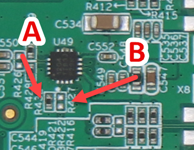
The default MUX1 resistor state is as shown in the figure, where the resistor at position A selects the 122.88MHz voltage-controlled oscillator, and at position B selects the 48MHz voltage-controlled oscillator.
For MUX2, its position is shown in the figure below:
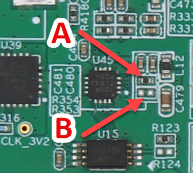
The default MUX2 resistor state is as shown in the figure, where the resistor at position A selects the 156.25MHz crystal oscillator, and at position B selects the LMK04828 chip.
LMK04828 is connected to the PL side through SPI bus. All control interfaces connected to the PL side are defined as:
| Interface Name | Interface Pin (S) |
|---|---|
| SDIO | B11 |
| SCK | G11 |
| CS | A10 |
| SYNC | A12 |
| RESET | B12 |
| CLKIN_SEL0 | E12 |
| CLKIN_SEL1 | D12 |
| STATUS_LD1 | G13 |
| STATUS_LD2 | H13 |
For methods and suggestions on clock tree configuration, please refer to Clock Tree Configuration Suggestions
¶ Power
The board is powered through a DC-044A interface. The power input voltage should be 12V DC, and the current should not be less than 5A. The board provides ample power supply of 0.85V@50A for the FPGA core, and also uses different IO voltages for different IO Banks. Details are shown in the table below:
When the chip's logic design has high power consumption, please ensure sufficient thermal margin, otherwise the board may be damaged. For specific suggestions, please refer to Thermal Suggestions.
| IO Bank | Voltage |
|---|---|
| PL BANK 65 | 1.2V |
| PL BANK 66 | 1.2V |
| PL BANK 88 | 3.3V |
| PL BANK 89 | 3.3V |
| PS BANK 500 | 1.8V |
| PS BANK 501 | 1.8V |
| PS BANK 502 | 1.8V |
| PS BANK 503 | 1.8V |
| PS BANK 504 | 1.2V |
PS BANK 502 is connected to the Ethernet PHY chip, so it supports multiple level modes. The board defaults to 1.8V, and can also be modified to 3.3V by changing the configuration resistor.